

At high-tech Eindhoven, groundbreaking technology is being developed, enabling scientists to make exciting new discoveries. Thermo Fisher (formerly Fei) develops and assembles electron microscopes there that can push the boundaries of the laws of physics. Sentech is allowed to contribute to two important components of the Talos™ and Krios™ transmission electron microscopes (TEMs), namely the Aperture mechanism and the Compustage.
For this, the Eindhoven company, acquired by Thermo Fisher in 2016, has relied on Sentech's sensor knowledge for 15 years. Thermo Fisher is even one of the reasons for Sentech's founding. Sensor technology ensures that the electron beam lands exactly on a specimen and that the specimen is in the correct zero position.
It can't be long now before the Eindhoven nanotechnology of Thermo Fisher, with sensor technology from Sentech, leads to the next scientific breakthrough.
Scientific research at the nanometer scale
Sentech's origin story is closely linked to Thermo Fisher. The company develops and produces high-quality technology for scientific research and diagnostics.
Thermo Fisher complements this technological spectrum with microscopy for nanometer and even picometer research. For microscopic research on the smallest scale, the company develops the most advanced and extremely powerful electron microscopes.
The TEM (Transmission Electron Microscope) and SEM (Scanning Electron Microscope) image samples down to the sub-nanometer level. A scale that is barely imaginable. They make individual atoms and molecules visible.
What was previously invisible to humans can now be visualized in high resolution. Thermo Fisher's electron microscopes literally defy the ultimate boundaries of our universe.
It's no wonder that groundbreaking scientific discoveries are being made with Thermo Fisher microscopes. Nature has declared cryo-electron microscopy (cryo-EM) as the ‘Method of the Year 2015,’ a microscopy technique that can only be performed with Thermo Fisher microscopes (Krios™).
For the first time in history, scientists can examine protein structures (RNA and DNA) at a molecular and atomic level. Scientists from universities and pharmaceutical companies expect to develop new medicines and treatment methods for diseases from this.
Thermo Fisher microscopes are also crucial for semiconductor research, mineral research, industrial research, and other nanometer-level research.
Sentech sensors crucial for TEM electron microscope
The Krios™ TEM It is three meters high and is assembled in Eindhoven using components from various suppliers. A beam of electrons is sent down through a column of electronic ‘lenses’ towards the sample. The material to be examined is located on the 4-axis stage (Compustage).
A portion of the electrons are absorbed by the material. The passing electrons then form a ‘still image’ of the sample in the image acquisition and detection unit. Software translates the images into a two- and/or three-dimensional high-resolution image of the material.
The TEM consists of several main components that are precisely integrated into the assembly. For a perfect image of a protein structure or the surface of a semiconductor, it is crucial that the sample is positioned in the correct spot within the electron beam by the Compustage.
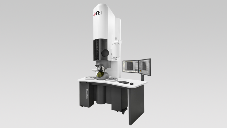
Titan Halo microscope with Sentech sensor technology
Sentech's sensor technology has ensured the stability and correct positioning of this stage for 15 years. And for the control of the aperture mechanisms, which precisely direct the electron beam towards the sample.
Sentech stepped into the sensor gap left by Honeywell when it divested its sensor product line. The company developed two types of sensor assemblies for the TEM versions.
The inductive sensors provide homing (returning to the starting point) or detection of the stage, depending on the application. The proximity sensor indicates whether the stage is present in the vacuum chamber. This sensor prevents the chamber from remaining open during vacuum evacuation.
The microscope contains multiple aperture mechanisms. These position the aperture in the electron beam. Sentech supplies the sensor assemblies with inductive sensors to first-tier suppliers, including Frencken. Frencken manufactures and supplies the aperture mechanism.
Partnership – improvements through close collaboration
Sentech works closely with the operations engineers at Thermo Fisher in Eindhoven and with Frencken, the supplier of the Aperture mechanism. Sean Ram, account manager at Sentech, about the collaboration: “In the past 15 years, the development of the TEM has not stood still, particularly in the field of imaging. The cameras and images have improved enormously.”
Due to product changes at Thermo Fisher and advancements in sensor technology, several modifications have been made to the sensor assemblies. “We don't see ourselves as a sensor supplier, but as a sensor integrator who collaborates with our clients. We feel like an R&D extension of Thermo Fisher. For example, recently the integrated circuit (IC) in certain sensors was replaced because the previous one was outdated.”
Professional supply chain guarantees high quality
Sentech supplies its sensor assemblies (including wiring) on a just-in-time basis. Ram: “Sentech adheres to an extremely high quality standard that we have secured throughout the entire chain, from development to distribution. Only in this way can you meet the high quality requirements of high-tech clients like Thermo Fisher.”
The quality mindset is ingrained in all employees. “This also means that we deliver exactly to the right place and at the right time when sensor assemblies are needed in the production and assembly process. We cannot afford mistakes. The entire supply chain is advanced and optimally regulated, including a cleanroom with production, testing, and packaging facilities,” Ram concludes.
You optimize your machine like this with sensor integration
It won't be long before the Eindhoven nanotechnology from Thermo Fisher, with sensor technology from Sentech, brings about the next scientific breakthrough. Big data will then be indispensable in making your machine smarter.
Based on customer needs and the future outlook, you determine what data you need. Furthermore, you need the right sensor solution to collect big data.
What can you expect from technologies? Let us inspire you free e-book.
Brainport Eindhoven, a melting pot of high-tech companies, is home to a large number of Sentech's clients. These include OEMs within the semiconductor market and their specialized suppliers.
As their R&D partner, Sentech develops and supplies sensor integrations, often complete sensor assemblies: assies. In mid-2013, one of the module builders approached Sentech for a new OEM development.
As an R&D partner, Sentech has taken on this development. With its solution-oriented sensor and application knowledge, Sentech has already elevated many machines and precision technologies to a higher level.
The balance between the high demands of the semiconductor market and cost is a challenge.
The semiconductor industry revolves around precision mechanics and mechatronics. High-tech machines are used in cleanrooms to deposit extremely thin layers of material onto a substrate (wafer). Sentech develops high-quality sensor technology in the form of fully integrated sensor assemblies for, among others, ASML machines and various ASML suppliers.
These sensor solutions control and monitor transport processes to, within, and out of process areas, among other things. This yields valuable information with which the semiconductor industry can improve its machines and subsystems. Precision work at the nanometer level results in high quality requirements for all components of these systems.
This is contrasted by the need to keep costs acceptable, according to Peter Verstappen, account manager at Sentech. “Almost anything or a lot is possible, but that comes at a cost. Sentech feels right at home in that balance between technical and commercial feasibility. We find it challenging to develop the most optimal sensor solutions within an acceptable budget.”
Sentech's starting points are the client's problem statement and challenge.
Sentech regularly receives requests from semiconductor OEMs and their suppliers to be their R&D support. Verstappen: “We brainstorm with them about the sensor challenges in their designs. You mainly have to think about detecting, controlling, and measuring the transport process of wafers in and out of the process chambers.”
In the process rooms, the surface treatment of the wafer takes place. This requires extreme precision, but because the process occurs on such a small scale, it is not visible to the naked eye. Sensors are needed for positioning, controlling, and measuring the wafers.
Verstappen: “It starts with a functional requirements package for the process and function of a machine or system. We then translate that into mechatronics. Sentech then investigates which sensor technology is most suitable for control, steering, and measurement. It's about finding the sweet spot.”
Which sensor technology is best suited for this challenge? “Only then do we think about the form of a sensor. The integrated costs naturally play an important role in this.”
Semicon – sensors for transport, positioning, detection, and measurement
In the manufacturing processes of semiconductor machines, we distinguish several processes that are controlled, regulated, and measured by sensors. The first process is the feeding of semi-finished products into the machine. Sensors are needed to reliably select, detect, and then transport the products to the machine.
In the next step, surface treatment takes place in a process chamber. The temperature, any vacuum present, and any process gases will determine the sensor technology required there. In the final process step, the end product is moved from the process chamber to the appropriate location for further processing.
Verstappen: “In this case, selecting and developing the right sensor technology for the process space was the biggest challenge. The closer you get to the primary processing operation, the higher the temperature becomes. Normally, sensors and their internal electronics can withstand temperatures up to around 70°C. For this OEM's process space, we had to use sensors that can withstand temperatures up to 140°C.”
The process chamber currently contains temperature-resistant inductive proximity switches. “We also had to take into account special light wavelengths that cause most materials to age and degrade significantly. Sentech's extensive experience makes them knowledgeable in this area. For this application, we sought the best fit on the market in relation to the functional requirements and integration costs. We always try to find standard off-the-shelf sensor products for the assemblies, as development is not an end in itself.”
What is a wish and what is a requirement are crucial questions to ask to arrive at the most suitable solution. “For this client, sensor integration of standard components that were immediately deployable was the outcome for most positions. At a number of locations, we adapted the sensor's design to environmental requirements or dimensions. This led to a temperature-resistant proximity switch, including cabling and connector, and a temperature sensor in a special housing.”
In total, seven different sensor technologies were used for this client, including: optical and inductive sensor technology, temperature sensors, O₂ sensors, optical encoders, fiber optic sensors, and non-contact radiation sensors (pyrometers).
R&D partner for semiconductors: working on sensor integration
Sentech works for many players in the Dutch semiconductor market. These are mainly concentrated in the three technology regions, where, not entirely by coincidence, the Technical Universities are also located.
Verstappen: “With this module builder, we started OEM development in 2013. After a relatively quiet intervening year, we were asked in mid-2015 to support the next development steps. Sentech now supplies a variety of sensors and assemblies used in these machines. As their R&D partner, we organize meetings with the involved engineers and system architects at essential moments. We do this to prevent email ping-pong and to avoid leaving interpretations to chance.”
Sentech takes the initiative in sensor development. “Our customers tell us that we are truly unique in this. The meetings contribute to the focus on technological and financial feasibility. And that's how we maintain momentum.”
For this client, there was still much to gain after the initial design, as not all sensor functions were yet delivered as completely validated sensor assemblies. “An assembly has many advantages: it ensures higher reliability because Sentech can test and perfect the complete assembly. Working with assemblies makes modular construction and assembly of the machines possible, which, in addition to guaranteeing quality, also results in a faster turnaround time,” explains the account manager.
Added value for high-tech manufacturers
In complex high-tech development processes, Sentech's added value truly comes into its own. Verstappen: “The more complex the technological challenge, the more necessary a sensor expert is. Sentech shines in such development processes. Where the large sensor manufacturers have to drop out, we can provide the best solutions at acceptable costs. We love technically complex questions and challenges.”
Furthermore, Sentech is very transparent with its clients and presents clear alternatives. “But we are not just a reliable R&D partner. The reliability and quality of our production, testing, and distribution processes are just as high.”
What Verstappen says is confirmed by Sentech's variety of quality certificates from quality institutes.
Here's how to implement sensor technology
Integrating successful sensor technology presents challenges. How do you prepare for environmental factors you are not yet aware of? And what sensor trends can you expect in the future as an engineer?
In our free e-book, you'll find answers to these, including practical examples of common sensor issues and solutions.